
Two-dimensional materials have become the focus of extensive research due to their unique properties that differ from their bulk counterparts. These materials, consisting of only one or two layers of molecules, exhibit a range of characteristics that can be controlled and manipulated for various applications.
A research team led by physicist Prof. Ursula Wurstbauer has been delving into the ways in which the properties of two-dimensional crystals can be controlled to exhibit specific behaviors such as insulating, conducting, superconducting, or ferromagnetic. By exploring the interactions between charge carriers (electrons) and the energy landscape of the crystals, the team has made significant strides in understanding and influencing these materials.
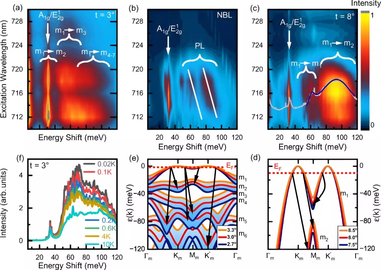
In a groundbreaking study published in Physical Review Letters, the team has successfully generated and quantitatively demonstrated collective excitations of charge carriers within different energy landscapes. This achievement has shed light on the electronic characteristics of crystal structures and unveiled new avenues for manipulation.
To achieve diverse properties in two-dimensional crystals, the scientists stacked two layers of a material on top of each other and twisted them slightly, creating moiré patterns. These geometric patterns alter the energy landscape, causing electrons to move more slowly and interact intensely with each other. This phenomenon, known as strongly correlated behavior, is essential in understanding the behavior of electrons in these unique structures.
The use of two-dimensional materials goes beyond fundamental research, as Prof. Wurstbauer points out. These materials hold promise for innovative applications in quantum technology, neuromorphic components, and circuits. The ability to manipulate the properties of these materials opens up a realm of possibilities for future technological advancements.
Collaborating with scientists from various institutions, including the University of Hamburg, RWTH Aachen University, and the Max Planck Institute for the Structure and Dynamics of Matter in Hamburg, Wurstbauer’s research group conducted a series of experiments. By preparing and analyzing different two-dimensional crystals like graphene, molybdenum diselenide, and tungsten diselenide using optical spectroscopy methods at cryogenic temperatures, the team gained valuable insights into the behavior of these materials.
The study of two-dimensional materials continues to unveil new perspectives on material properties and their potential applications. The ability to control and manipulate these materials at the atomic level opens up exciting possibilities for the future of technology and innovation. As researchers delve deeper into the complexities of these materials, we can expect to witness groundbreaking advancements in various fields.
Leave a Reply