
Recent advancements in semiconductor research at UC Santa Barbara have unveiled a groundbreaking achievement: the first visualization of electric charges traversing the interface of two distinct semiconductor materials. This pioneering work, spearheaded by Professor Bolin Liao and his team through the innovative scanning ultrafast electron microscopy (SUEM) methods, provides unprecedented insight into a phenomenon long discussed in theoretical frameworks but rarely captured in direct observation. By making the invisible aspects of semiconductor physics visible, this research paves the way for a deeper understanding of carrier dynamics that play a crucial role in various applications, including solar energy, lasers, and sensors.
Understanding the behavior of photocarriers—the charge carriers generated when sunlight excites electrons in semiconductor materials—is vital for optimizing technologies that rely on these materials. In practical applications, like solar cells, photons from sunlight energize electrons, allowing them to move and generate an electric current. Despite their potential to initially carry substantial energy, these excitations, or “hot carriers,” dissipate most of their energy rapidly, within picoseconds. Unfortunately, this means that only a fraction of the potential energy can be harnessed for practical use, posing challenges in harnessing solar energy efficiently.
The significance of studying hot carriers becomes apparent when considering their implications for device performance. Understanding how these carriers behave, particularly at the interfaces between different materials—known as heterojunctions—is crucial for improving the efficiency of technological applications such as photovoltaics and laser diodes. The complete integration of theory with direct observational techniques offers a new lens through which semiconductor researchers can address fundamental questions regarding energy loss and carrier mobility.
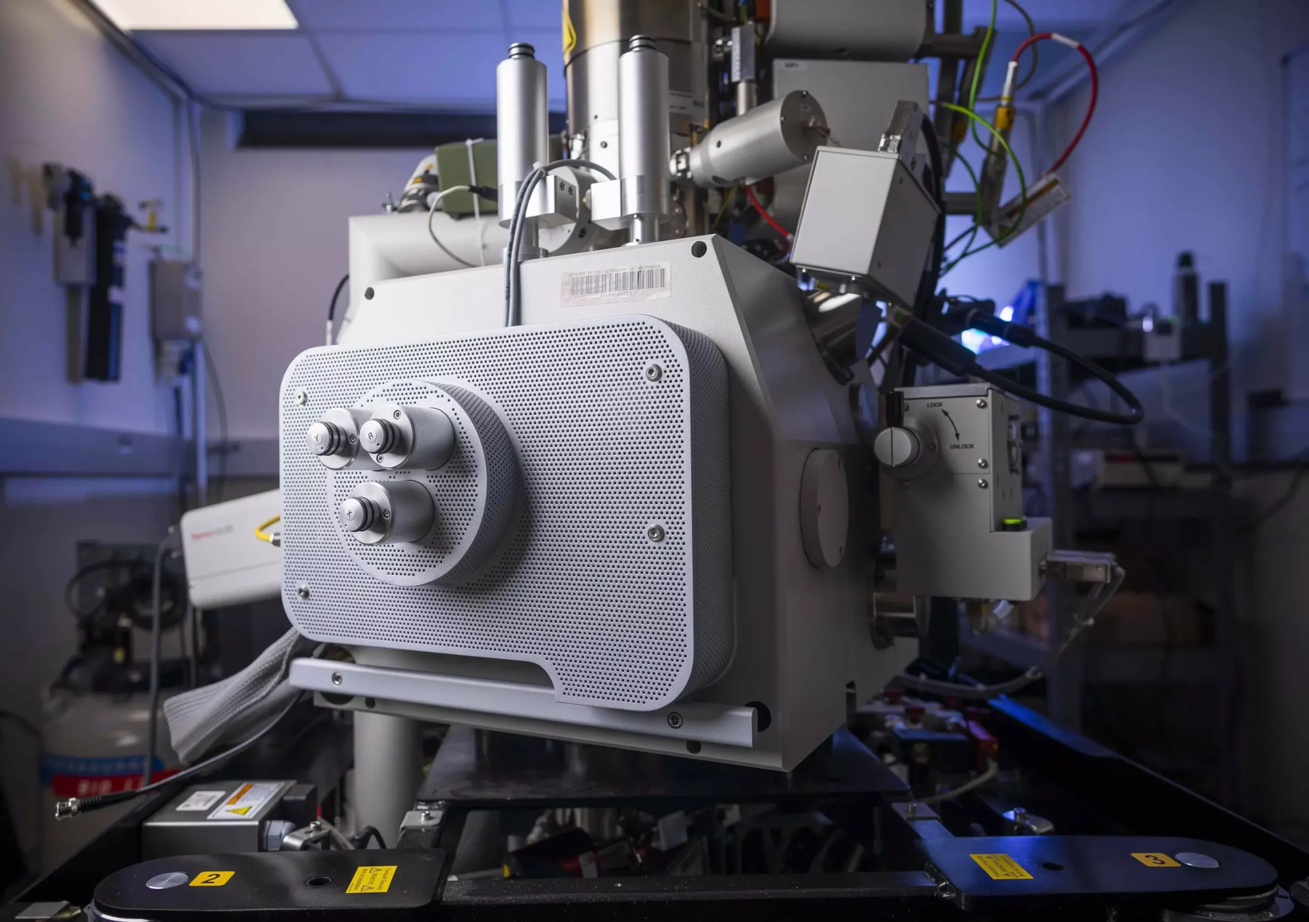
At the heart of this research is the SUEM technique, which integrates ultrafast laser pulses to create a “shutter” that provides temporal resolution on the order of picoseconds. This revolutionary approach allows researchers to capture the fleeting moments when charge carriers are generated and begin traversing the semiconductor interface, essentially freezing a dynamic process that traditionally evaded direct observation. By utilizing an electron beam to scan the newly formed photocarriers excited by an optical pump, Liao’s team was able to create instantaneous images of their movements.
The implications of this imaging breakthrough are vast. Traditional semiconductor research has often relied on indirect measurements, which, while informative, can’t capture the real-time behavior of these charge carriers. Liao highlights that this achievement is not merely an academic interest; it serves as a critical tool for semiconductor scientists to benchmark existing theories and refine their understanding through direct empirical evidence.
The findings revealed how photocarriers behave differently when generated in uniform regions of silicon or germanium versus those generated near heterojunctions. Notably, carriers excited at the junction experience a slowing effect due to charge trapping caused by the junction’s potential. This observation underscores the complexity inherent in semiconductor design: while theoretical models suggest these behaviors, direct observations provide concrete evidence that could inform strategies to mitigate carrier trapping issues that detrimentally affect device performance.
The discovery correlates directly with the foundational theories established by the late Professor Herb Kroemer, who conceptualized the importance of heterostructures within semiconductors. His maxim that “the interface is the device” resonates now more than ever as the interplay between materials at their junctions continues to dictate advancements in semiconductor technology.
The ability to visualize hot carrier dynamics at heterojunctions opens new avenues for research and development within the semiconductor field. Armed with this capability, scientists can now develop more efficient photovoltaic systems, enhanced laser technologies, and improved sensors. By illuminating the behavior of carriers at interfaces, researchers can explore tailored material designs that maximize charge transport and efficiency.
Moving forward, enhancing the SUEM methodology and applying it to a broader range of materials and device architectures will be crucial. As technology increasingly demands higher performance in faster, more efficient devices, understanding how to control and optimize the behavior of carriers at the microscopic level will be imperative.
The recent achievement at UC Santa Barbara represents a significant step in bridging the gap between theoretical models and real-world applications in semiconductor science. By visualizing how electric charges move across interfaces, researchers can better understand and innovate the devices that shape our technological landscape today. As we strive to harness and optimize the power of semiconductors, such foundational research will undoubtedly lead to more efficient and advanced technologies that could define the future.
Leave a Reply