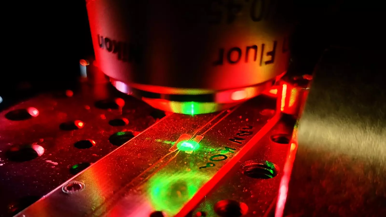
In a groundbreaking development in the field of quantum technology, researchers at TMOS and RMIT University have unveiled a new 2D quantum sensing chip using hexagonal boron nitride (hBN). This innovative chip, detailed in a paper published in Nature Communications, has the remarkable ability to simultaneously detect temperature anomalies and magnetic fields in any direction, all within a thin-film format. The implications of this new technology could revolutionize the quantum sensing industry, making sensors more versatile and cost-effective.
Traditional quantum sensing chips have been predominantly made from diamond, known for its robustness. However, diamond-based sensors have inherent limitations, particularly in their ability to detect magnetic fields. These sensors can only detect magnetic fields when aligned in the direction of the field, leading to significant blind spots when unaligned. This constraint necessitates the use of multiple sensors with varying degrees of alignment, complicating their operation and reducing their versatility in different applications.
Introducing Hexagonal Boron Nitride Sensing Chips
The research team led by TMOS Associate Investigator Jean-Philippe Tetienne and Chief Investigator Igor Aharonovich has taken a bold step towards a new quantum sensing platform using hBN. Unlike diamond, hBN crystals consist of atomically thick sheets that are flexible, allowing the sensing chips to conform to the shape of the sample under study. This flexibility enables the hBN sensors to get much closer to the sample, overcoming a limitation of diamond-based sensors.
The Discovery of a New Carbon-based Defect
One of the key breakthroughs in this research is the identification of a carbon-based defect in hBN that exhibits a half spin system, enabling the detection of magnetic fields in any direction. By conducting Rabi measurement experiments and comparing the results with the well-understood boron vacancy defect in hBN, the researchers were able to characterize this new defect’s behavior. The unique properties of this defect allow for electrical excitation control, similar to the boron vacancy defect, opening up new possibilities for quantum sensing applications.
The development of hBN quantum sensing chips holds great promise for a wide range of applications, including the in-field identification of magnetic geological features and radio spectroscopy across a broader bandwidth. The 2D form factor of hBN sensors, coupled with their directional independence, makes them ideal for applications in dynamic environments, such as biological systems. The cost-effectiveness and accessibility of hBN compared to diamond further enhance its potential for widespread adoption in various industries.
The emergence of 2D hexagonal boron nitride quantum sensing chips marks a significant advancement in the field of quantum technology. The unique properties of hBN, combined with the discovery of a novel carbon-based defect, have paved the way for more versatile and efficient quantum sensors. As researchers continue to explore the potential applications and fine-tune the performance of hBN sensors, we can expect to see a new era of quantum sensing technologies that will revolutionize various industries.


Leave a Reply