Antiferromagnets represent a fascinating class of materials whose magnetic properties defy conventional magnetism seen in ferromagnets. In these materials, the magnetic moments of neighboring atoms manifest in an alternating pattern—think of them as polar opposites in a dance that cancels each other out. This unique arrangement leads to the absence of net macroscopic magnetism, while still allowing for intricate electronic phenomena. As this field garners attention from researchers, the potential applications in burgeoning technologies—particularly in spintronics—become ever more appealing.
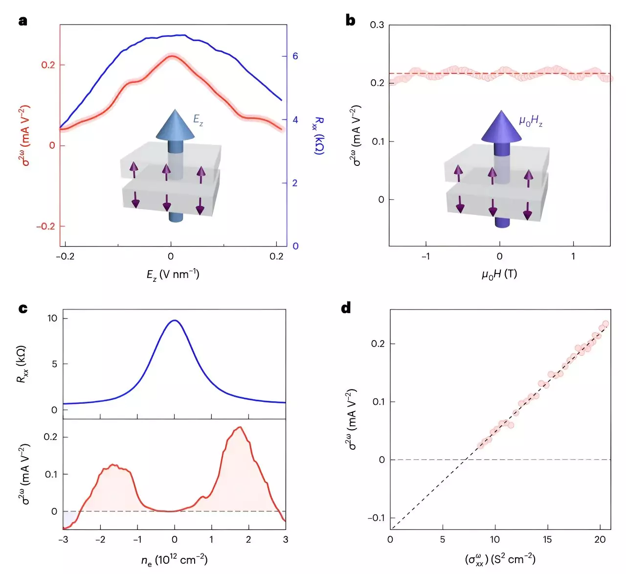
Recently, a team of researchers at Harvard University unveiled a significant breakthrough concerning the antiferromagnetic material MnBi2Te4, composed of even-numbered layers. Their investigation centered on the observation of an antiferromagnetic diode effect, a phenomenon that could serve as a springboard for innovations in electronic design. Unlike conventional diodes that harness asymmetric charge flow, this antiferromagnetic variant exists in a centrosymmetric crystal structure, challenging our understanding of charge separation dynamics.
This pivotal research has been published in the esteemed journal Nature Electronics, opening up new avenues for device applications such as in-plane field-effect transistors and systems designed for microwave energy harvesting. Significantly, the diode effect they identified enables the controlled flow of electrical current in a single direction, a principle not only foundational to electronic devices such as radio receivers and temperature sensors but one that could be transformed in new configurations.
To investigate the antiferromagnetic diode effect in MnBi2Te4, the Harvard team utilized sophisticated fabrication methods to create devices with distinct electrode configurations. Employing both Hall bar and radially distributed electrodes enabled them to measure nonlinear electrical transport characteristics effectively. Their experimentation led to confirmed evidence of the antiferromagnetic diode effect, demonstrating its potential across devices configured differently.
The methodology employed by the researchers was diverse, incorporating spatially resolved optical techniques and electrical sum frequency generation (SFG) measurements. Their observations revealed considerable second-harmonic transport, indicating complex nonlinear responses facilitated by the material’s compensated antiferromagnetic state.
The implications of these findings extend far beyond laboratory exploration. “We show that this antiferromagnetic diode effect can be used to create in-plane field-effect transistors and microwave-energy-harvesting devices,” stated the research team’s authors, highlighting the practical applications these findings could have on evolving technology landscapes.
As the significance of the antiferromagnetic diode effect becomes more pronounced, it raises intriguing questions about its implementation in future electronic devices. The prospects for antiferromagnetic logic circuits, microwave energy harvesters, and advanced spintronic technologies illustrate just a fraction of its potential.
The research emphasizes that the newfound diode effect could prompt further investigations into quantum materials and their unique properties. This interplay between theoretical understanding and practical application underscores a critical turning point for materials science research, where curiosity drives innovation.
As the study encourages others in the scientific community to explore the bounds of antiferromagnetic materials, it also sets the stage for interdisciplinary collaboration. Engaging physicists and engineers alike, this invites fresh perspectives that may lead to a better understanding of these materials.
The Harvard team’s exploration of the antiferromagnetic diode effect marks an exciting juncture in material science, particularly within the domains of electronics and spintronics. The confirmation of this effect in a centrosymmetric crystal showcases not only the versatility of antiferromagnetic materials but also the potential they hold for future technologies. As researchers continue to peel back layers of complexity in materials like MnBi2Te4, we may be ushering in new forms of electronic devices that challenge the conventional paradigms currently guiding our technological advancements. Ultimately, this signifies a bold step towards harnessing quantum materials for practical benefits, propelling us into a new age of innovation.


Leave a Reply