
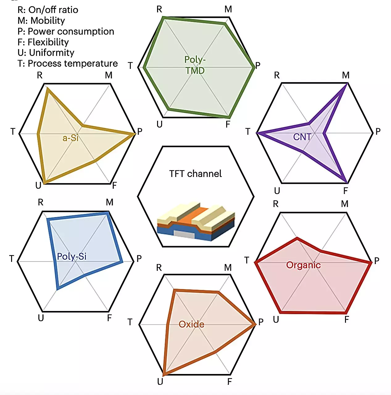
In the quest for designing more advanced and scalable transistors, electronics engineers have been exploring alternative materials with higher electron mobility. Transition metal dichalcogenides, particularly molybdenum disulfide (MoS2), have emerged as promising candidates for the development of field-effect transistors (FETs) due to their small length and good carrier mobility. Recent research conducted by a team of researchers from Samsung Advanced Institute of Technology (SAIT) and Seoul National University has showcased a significant breakthrough in integrating MoS2 transistors on a 200 mm wafer.
The team first fabricated large-scale arrays of MoS2 FETs using metal-organic chemical vapor deposition (MOCVD) to eliminate the Schottky barrier at the interface between the MoS2 material and metal. This novel fabrication strategy not only enhanced the FETs’ carrier mobility but also allowed for compatibility with current electronics manufacturing processes, achieving an impressive yield of over 99.9%.
The MoS2 FETs developed by the researchers exhibited remarkable performance characteristics, surpassing previously introduced MoS2-based FETs in terms of field-effect mobility, contact resistance, and on-current densities. With mobilities of 21 cm2 V-1 s-1, contact resistances of 3.8 kΩ·µm, and on-current densities of 120 µA µm-1, these FETs demonstrated a significant improvement attributed to the elimination of the Schottky barrier and reduction in contact resistance.
Upon integration of the FETs on a 200 mm wafer, the researchers observed uniformity across the devices with minimal die-to-die variations, highlighting the scalability and reliability of the fabrication process at existing industrial facilities. The team’s achievement in 200-mm-wafer-scale integration of polycrystalline MoS2 FETs not only paves the way for the development of smaller and flexible devices but also sets a precedent for future research and commercialization efforts in the semiconductor industry.
The successful integration of MoS2 transistors on a 200 mm wafer represents a significant milestone in the advancement of semiconductor technology. By bridging the performance gap between single-device demonstrations and large-scale integration, this research opens up new possibilities for the development of high-performance transistors based on two-dimensional materials. The implications of this breakthrough extend beyond the realms of academic research, inspiring further exploration and experimentation in the field of semiconductor engineering. As we look towards the future, the integration of MoS2 FETs on a commercial scale holds immense promise for revolutionizing the electronics industry and shaping the landscape of technological innovation.
Leave a Reply