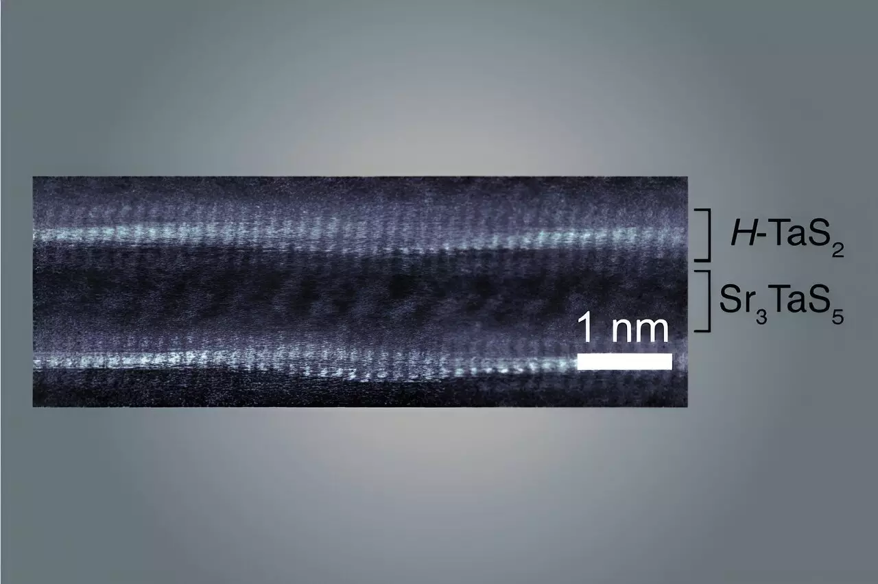
Recent advancements in material science have captured the attention of the scientific community, particularly concerning the development of novel superconducting and metallic materials. Researchers at MIT have pioneered this field by fabricating a unique substance characterized by undulating atomic layers just a few nanometers thick. This groundbreaking work presents a sizeable macroscopic sample, allowing for manual manipulation and an in-depth study of its quantum behaviors—interactions at the atomic level that dictate the material’s exceptional properties. The team’s findings, published in the prestigious journal Nature, highlight a significant breakthrough in materials engineering through rational design, a method that promises further discovery of materials with unprecedented characteristics.
The synthesis of this new material is more than just a stroke of luck; it stems from the researchers’ meticulous understanding of chemistry and materials science. By designing a systematic approach to assemble these layered structures, the physicists have turned theory into practice. As senior investigator Joseph Checkelsky notes, achieving a structured setup of uniform atomic layers opens up exciting opportunities to explore new physical properties. The potential of two-dimensional materials has captured attention due to their ability to be manipulated in ways that yield extraordinary characteristics. For instance, slight rotations, commonly referred to as “twists,” of these layers can create intricate moiré superlattices, leading to behaviors such as superconductivity and unconventional magnetism.
As reported, the new material created by the MIT team comprises alternating layers of tantalum and sulfur arranged atop a spacer layer made up of strontium, tantalum, and sulfur. This layered arrangement creates an atomic structure akin to a layer cake, with thousands of these corrugated layers stacked together to form a single crystal. What is particularly striking is the uniformity of these waves across the entire crystal, establishing a new standard in the design of layered materials.
Unlike other known materials with similar wavy structures, this new compound achieves a level of perfection in its atomic arrangement, a factor critical for consistent properties. The team hypothesizes that the ‘waves’ emerge due to the structural and size mismatches inherent in the different layers. This disparity creates a buckle-like phenomenon, where one layer accommodates the other, thus forming the sought-after waviness. This analogy can be compared to layering different-sized papers, where one must bend to overlay the other.
The implications of this waviness are profound, allowing the material to exhibit superconductivity when cooled to specific temperatures. At these critical points, electrons can flow freely without experiencing any resistance—an effect that arises, in part, from the structural undulation. Devarakonda elaborates on this, suggesting that the “waviness” of the material influences the electron’s behavior, allowing them to navigate through it more efficiently.
The researchers have effectively introduced a guiding directionality into the flow of electrons, whereby the newly created structure facilitates movement down the ‘troughs’ of the waves rather than across the ‘hills.’ This alteration could significantly impact the material’s metallic properties, potentially leading to innovative applications in the electronics and energy sectors. The discovery lays the groundwork for new avenues in material exploration; as Devarakonda aptly puts it, they have “planted the flag” for future research.
Moreover, the implications of synthesizing materials with identified properties through a systematic design could revolutionize how we approach material development in the future. By standing on the foundation built by previous researchers, this team has ventured into a largely uncharted territory filled with unexpected outcomes.
The emergence of this wavy layered material exemplifies the exciting possibilities that rational design can offer to the field of condensed matter physics. As researchers continue to delve deeper into the properties of materials at the atomic scale, the potential applications that could arise from this newfound knowledge are vast and varied. Whether in the realm of quantum computing, high-efficiency energy systems, or innovative electronics, the implications of this research could very well change the landscape of material science for years to come. With their pioneering spirit, the MIT team’s findings illuminate a path toward understanding and harnessing materials with extraordinary characteristics, unveiling a new frontier in superconductivity that holds promise for future generations.


Leave a Reply